Failed capacitors have a very high ESR that, even without measurement, should be pretty obvious once you've measured a few known good caps.
Testing Capacity
You can also tell if a capacitor has lost capacity if the Xc voltage drop is too high compared to a known good capacitor of the same value, or even other caps on the same board. Take a look at the difference between these two 100uF capacitors on my Hero Jr robot, below. Maybe this is due to wide value tolerance, or it could be due to aging.
 |
| Xc is much larger suggesting lower C |
 |
| Xc is a lot lower suggesting higher C |
Testing for Shorts
In the above pictures I had the scope on AC mode. To test for shorted capacitors, make sure the test waveform has a DC offset. Switch the scope to GND mode and set the position to coincide with the zero mark in the middle vertically. Then, switch to DC, and re-test your capacitors and make sure the lowest voltage across the cap is greater than zero (above the line).
Measuring ESR
From
Powell's website on ESR measurement, here are some heuristics for testing the health of capacitors:
- 1µF - 100µF : 0.7Ω ideal, up to 2Ω probably ok.
- > 100µF : anything over about 1Ω means a degraded capacitor.
Translating ohms to voltage drop to display divisions on the 'scope uncovered an issue with sensitivity of the circuit to low ESR, mentioned earlier. It could detect ridiculously high ESR but discerning between, say, 1Ω and 2Ω was a no go. One fix was using the correct value resistors.
Screwing Up Testing
In addition to using the wrong resistors, my oscilloscope probe was set to 10X (attenuating the signal by 10). After fixing the resistors and the probe, the circuit had good sensitivity to low ESR.
Quick Translation Table
How do you translate screen reading to ESR? I put together a table and graph to translate directly from waveform amplitude in 'scope divisions to ESR value.
Measuring amplitude out of pin 3 on the 555, and then calculating total resistance and thus current, it was possible to calculate voltage drop for various ESR capacitors in parallel with R5 (6.8Ω), then convert that to the number of divisions on the scope, when it's set to either 5mV/division or 10mV/divison.


The graph makes it easy to quickly read ESR based on amplitude of the waveform across a test capacitor. With the scope set to 10mV/division, here are the heuristics restated:
- 1µF - 100µF : 1.0 - 2.2 divisions probably ok.
- > 100µF : no more than 1.2 divisions
Be sure to adjust for your minimum test resistance by shorting your +/- probe leads. The final circuit showed a couple tenths of an ohm resistance, basically about 0.2 divisions. Just add 0.2 divisions to the above.
PCB Fabrication Tips
As before, I put together the schematic and board layout in Eagle. This time I used copper pour regions (polygons in Eagle) for ground so that less etching, and etchant, were necessary.

I found that soldering components to the big swaths of copper is tricky so next time I will try using "thermals" which adds some space around the pads to ensure most of the heat is directed at the pad (see below)
 Thermal pad isolation, detail
Screwing Up PCB Fabrication
As with my prior attempts at
DIY PCB etching, I found the method using magazine paper and clothes iron transfer is still a bit tough to get right. The magazine paper kept jamming in the laser printer. Also, it's important to let the transfer and board cool down before messing with it, otherwise you'll peel the magazine paper away and ruin the transfer. When ironing, the length of time and amount of pressure remains important. Too much pressure and time and the traces get blotchy. Too little time and the transfer isn't thorough. After a couple outright failures, I got a transfer that was good enough, but certainly not great.

 PCB after transfer (left) and after etching (right)
The etching method using Ferric Chloride with a sponge still takes forever. Frankly for all that scrubbing, I'd just as soon dump the board in a tank and let it sit for an hour (or however long it takes). Plus there would be less risk of spilling FeCl all over the garage floor (yes, my garage floor now has giant yellow spots), my clothes, hands, etc. I'll try that approach next time.
Drilling
Drilling went ok. I used the drill map approach from
last time wherein my Perl script converts a drill file into a CSV that can be imported and graphed in Excel or OpenOffice Calc. I again used a scatter plot in OpenOffice Calc to draw a diagram showing what drill sizes to use for each hole.
 Board Assembly
Most of the components I had on hand. For testing, I used bus wire to jumper out the variable resistors and a simple 9V connector for power. When I powered it up and connected to the scope, it displayed a waveform. As described above I had to fix some glitches to get it working right.

 The finished board (left) works (right)
Screwing Up Some More
The main probe BNC, on the schematic, wires in series with a 22kΩ resistor. I think it's another overvoltage protection feature. After building everything I discovered this resistor messes up the square wave sent to the scope and jacks up the signal at higher frequencies. I never caught this because I never tested this aspect of the circuit properly.
Either replace the 22kΩ with bus wire or relocate the probe BNC where R6 used to be (very close to the pretty signal across R5 the 6.8Ω). I took the latter approach and it worked out fine. That leaves the ringing to deal with for another time.
Enclosure Design
I find selecting the enclosure and figuring out the layout is the hardest and most tedious part of the design. Designing the ESR harness last time was a nightmare trying to figure out how to get all the controls and jacks to fit into a microscopic case. Unlike last time, I am not picking the enclosure solely based on the size of the electronics but rather one with plenty of room for switches, knobs, etc.
But selecting that enclosure still was a pain. Originally I wanted knobs to adjust duty cycle and frequency, jacks for probes, and BNC jacks for the test waveform and a trigger waveform (because the signal waveform is so small for low-ESR capacitors a separate trigger signal is helpful). That, and a power switch. But after all sorts of planning and finding the perfect case, selecting the knobs and power switch I wanted, I discovered that the case was unavailable and cases of similar dimensions cost a fortune.
So I settled on a 5"W x 2"H x 5"L cabinet,
Hammond #1598-BSGY.
I redesigned the front panel again, ditching the external duty adjustment, using a smaller knob for frequency, ditching the banana jacks (a BNC t-fitting can be used to connect probe, harness, and oscilloscope), and using a smaller power switch. I also made sure the candidate power supply transformer will fit if I go that route.
Front Panel Design
Designing the front panel is easier using a nice drafting program like Visio or Inkscape (Windows) or OmniGraffle (Mac), which makes it easy to draw shapes and set their dimensions and positions precisely. Even better if you can conveniently mark the centers of all your drill holes so you can just print out the design as a template for drilling. OmniGraffle makes this ridiculously easy to do.
 |
| Making the front panel |
The front panel is just laser printed on paper. Not pretty, but adequate. I used packing tape used to cover it and affix it to the front panel metal. It's certainly no worse than scrawling on the panel with a Sharpie.
Final Assembly
With the front panel in place, it was easier to locate an optimal spot for the circuit board. One option for mounting is to use plastic glue (e.g., SuperGlue), JB Weld, or another epoxy to affix plastic standoffs to the inside of the plastic case. Another option is to simply drill holes and mount the standoffs from below. That's what I did. You could also obtain the case datasheet and design your PCB to fit built in standoffs in the case.
For now I used a 9V battery mounted in a clip inside the case, but as you can see below, I left enough room for a 9VDC power supply PCB and transformer when I placed the main circuit board.
The front panel component wiring was a matter of following the schematic and wiring up the BNC connectors, potentiometer, and power switch. The indicator LED is simply wired in series with a 470Ω resistor to limit current from the battery and wired to the nearby switch to ensure it only comes on when the switch is on.
I used some 'feet' from an old, dead CD player to finish it off, buttoned it up and tested a few dozen electrolytic capacitors.
 Time to arm the robots! No, not for world takeover. I'm talking about robotic arms. Digging through the stack of old robot stuff I ran across a photocopy of this ancient, August, 1980 series from Radio-Electronics.
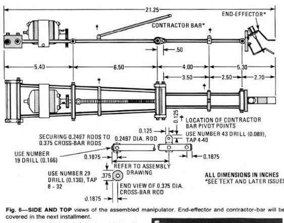 The elbow-forearm actuator is comprised of a large motor and threaded rod that pulls a on the midpoint of the forearm. The shoulder is actuated, I think, from a motor within the robot. Details on the design, dimensions, etc, are given below.
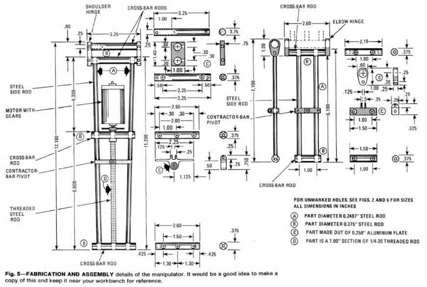 To save weight, I suppose one could change the design to use aluminum tube instead of steel rod for the side rods. They're available from home improvement stores, hardware stores, and online shops.
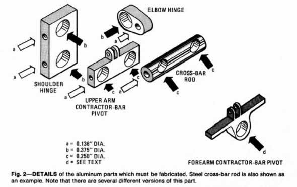 Some parts (right) need to be machined, unless one comes up with a simpler way to fabricate them. If so, I think all that's really needed is a drill press, a way to ensure drilling a hole through the center of a rod, a cutoff saw, some hand tools, and a tap or two.


